Sommaire L’aide du programme de gestion de base de données de ‘PElectro’ comporte la fenêtre suivante. Fenêtre Principale La fenêtre est la suivante : 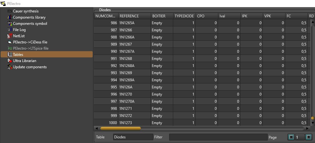
La fenêtre est composée d’une gestion de base de données. La gestion de base de données "DBPElectro.db3", permet de sélectionner une table. Les tables disponibles sont: - "Diodes" pour les diodes, - "Transistors" pour les transistors, - "Tec" pour les transistors à effet de champ. - "Mos" pour les Mosfet,
- "IGBT" pour les transistors bipolaire à grille isolée.
- "GasFet" pour les transistors à effet de champ à l'arséniure de gallium.
- "TFET" pour les transistors à effet de champ à grille métal-oxyde.
- "HFET" pour les transistors à effet de champ à hétérojonction.
Le choix peut se faire sur une partie du nom de la table. L’ouverture de la table se fait par le bouton 'Ouvrir’.
Le premier champ des fichiers ici NUMCOMPO doit commencer à 1 et s’incrémenter de 1 en 1. Un Utilitaire de saisie (Saisies) permet de créer, de modifier les enregistrements. Les bases de données utilisées par le Programme d’électronique “PElectro” sont : - Les Diodes dont la structure figure dans cette aide. - Les Transistors dont la structure figure aussi dans cette aide. - Les Transistors à effet de champ dont on trouve la structure dans l’aide. - Les Transistors MOS dont la structure est donnée dans l’aide.
- Les Transistors bipolaire à grille isolée dont les caractéristiques sont données dans l’aide.
- Les Transistors à effet de champ à l'arséniure de gallium dont les caractéristiques sont données dans l’aide.
- Les Transistors à effet de champ à grille métal-oxyde dont les caractéristiques sont données dans l’aide.
- Les Transistors à effet de champ à hétérojonction dont les caractéristiques sont données dans l'aide.
Structure de la base de données des diodes TYPEDIODE 1: Diodes normales, 2: Zener, 3: Schottky, 4: Tunnel, 5: Varicap et 6: Photoréceptrice. La signification des champs est la suivante pour les diodes normales, Zener, Schottky, Varicap et Photoréceptrice :
Diode
Forme générale D<nom> <(+) nœud> <(-) nœud> <nom du modèle> [area value]
Exemples
DCLAMP 14 0 DMOD
D13 15 17 SWITCH 1.5
Formulaire du modèle
.MODEL <nom du modèle> D [paramètres du modèle]
La liste des paramètres du modèle est donnée ci-dessous :
| Nom | Libellé du paramètre | Unité | Défaut | | AF | flicker noise exponent | - | 1.0 | | BV | reverse breakdown knee voltage | volt | infinite | | CJO | zero-bias p-n capacitance farad | - | 0.0 | | EG | bandgap voltage (barrier height) | eV | 1.11 | | FC | forward-bias depletion capacitance coefficient | - | 0.5 | | IBVL | low-level reverse breakdown knee current | amp | 0.0 | | IBV | reverse breakdown knee current | amp | 1E-10 | | IKF | high-injection knee current | amp | infinite | | IS | saturation current | amp | 1E-14 | | ISR | recombination current parameter | amp | 0.0 | | KF | flicker noise coefficient | - | 0.0 | | M | p-n grading coefficient | - | 0.5 | | N | emission coefficient | - | 1.0 | | NBV | reverse breakdown ideality factor | - | 1.0 | | NBVL | low-level reverse breakdown ideality factor | - | 1.0 | | NR | emission coefficient for isr | - | 2.0 | | RS | parasitic resistance | ohm | 0.0 | | TBV1 | bv temperature coefficient (linear) | °C-1 | 0.0 | | TBV2 | bv temperature coefficient (quadratic) | °C-2 | 0.0 | | TIKF | ikf temperature coefficient (linear) | °C-1 | 0.0 | | TRS1 | rs temperature coefficient (linear) | °C-1 | 0.0 | | TRS2 | rs temperature coefficient (quadratic) | °C-2 | 0.0 | | TT | Reverse recovery time | sec | 0.0 | | T_MEASURED | measured temperature | °C | 27 | | VJ | p-n potential | volt | 1.0 | | XTI | IS temperature exponent | - | 3.0 | | IVAL | valley point current (tunnel diode) | amp | 0.0 | | IPK | Peak point current (tunnel diode) | amp | 0.0 | | VPK | Peak point voltage (tunnel diode) | volt | 0.0 | | VVAL | Valley point voltage (tunnel diode) | volt | 0.0 | | θj | Maximum junction temperature | °C | 175 | | POWER | power dissipation in package | W | 0.0 | | RJTA | Junction to ambient thermal resistance | °C/W | 0.0 | | IFMAX | Forward current maximum | amp | 0.0 | | L | Channel length (photodiode) | meter | 1µ | | TF | Forward recovery time | sec | 0.0 | | IPH | incident photon flux (photodiode) | W/meter | 0.0 | | LAMBDA | Electromagnetic spectrum wavelength range (photodiode) | meter | 0.55 | | NA | The amount of acceptor atoms( photodiode) | Meter-3 | 1E24 | | TP | Mobility (photodiode) | meter²/Volt sec | 0.045 | | TPE | Mobility temperature exponent (photodiode) | - | 2.3 | | MFG | Manufacturer | - | - | La signification des champs est la suivante pour les diodes Tunnel : CP Courant de pic (Ipic). PN0 Courant de vallée (Ival). E Capacité parasite en Farad. A Constante marquant la pente de résistivité négative. UBR Tension de pic (Vpic). URM Tension de vallée (Vval). RD Résistance des contacts en Ohms. 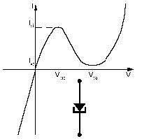
Formules des diodes
Structure de la base de données des Transistors La signification des champs est la suivante pour les Transistors :
Transistor bipolaire
Forme générale Q<nom> <nœud collecteur> <nœud de base> <nœud émetteur>
+ [nœud de substrat] <nom du modèle> [area value]
Exemples
Q1 14 2 13 PNPNOM
Q13 15 3 0 1 NPNSTRONG 1.5
Q7 CV 5 12 [SUB] LATPNP
Formulaire du modèle
.MODEL <nom du modèle> NPN [paramètres du modèle]
.MODEL <nom du modèle> PNP [paramètres du modèle]
.MODEL <nom du modèle> LPNP [paramètres du modèle]
TRANTYPE 1 pour NPN et 2 PNP.
Nom |
Libellé du paramètre |
Unité |
Défaut |
AF |
flicker noise exponent |
- |
1.0 |
BF |
ideal maximum forward beta |
- |
100.0 |
BR |
ideal maximum reverse beta |
- |
1.0 |
CJC |
base-collector zero-bias p-n capacitance |
farad |
0.0 |
CJE |
base-emitter zero-bias p-n capacitance |
farad |
0.0 |
CJS (CCS) |
ubstrate zero-bias p-n capacitance |
farad |
0.0 |
CN |
quasi-saturation temperature coefficient for hole mobility |
- |
2.42 NPN 2.20 PNP |
D |
quasi-saturation temperature coefficient for scattering-limited hole carrier velocity |
- |
0.87 NPN 0.52 PNP |
EG |
bandgap voltage (barrier height) |
eV |
1.11 |
FC |
forward-bias depletion capacitor coefficient |
- |
0.5 |
GAMMA |
epitaxial region doping factor |
- |
1E-11 |
IKF (IK) |
corner for forward-beta high-current roll-off |
amp |
infinite |
IKR |
corner for reverse-beta high-current roll-off |
amp |
infinite |
IRB |
current at which Rb falls halfway to |
amp |
infinite |
IS |
Transport saturation current |
amp |
1E-16 |
ISC (C4) |
† base-collector leakage saturation current |
amp |
0.0 |
ISE (C2) |
† base-emitter leakage saturation current |
amp |
0.0 |
ISS |
substrate p-n saturation current |
amp |
0.0 |
ITF |
transit time dependency on Ic |
amp |
0.0 |
KF |
flicker noise coefficient |
- |
0.0 |
MJC (MC) |
base-collector p-n grading factor |
- |
0.33 |
MJE (ME) |
base-emitter p-n grading factor |
- |
0.33 |
MJS (MS) |
substrate p-n grading factor |
- |
0.0 |
NC |
base-collector leakage emission coefficient |
- |
2.0 |
NE |
base-emitter leakage emission coefficient |
- |
1.5 |
NF |
forward current emission coefficient |
- |
1.0 |
NK |
high-current roll-off coefficient |
- |
0.5 |
NR |
reverse current emission coefficient |
- |
1.0 |
NS |
substrate p-n emission coefficient |
- |
1.0 |
PTF |
excess phase @ 1/(2π·TF)Hz |
degree |
0.0 |
QCO |
epitaxial region charge factor coulomb |
- |
0.0 |
QUASIMOD |
quasi-saturation model flag for temperature dependence if QUASIMOD = 0, then no GAMMA, RCO, VO temperature dependence if QUASIMOD = 1, then include GAMMA, RCO, VO temperature dependence |
- |
0 |
RB |
zero-bias (maximum) base resistance |
ohm |
0.0 |
RBM |
minimum base resistance |
ohm |
RB |
RC |
collector ohmic resistance |
ohm |
0.0 |
RCO |
‡ epitaxial region resistance |
ohm |
0.0 |
RE |
emitter ohmic resistance |
ohm |
0.0 |
TF |
ideal forward transit time |
sec |
0.0 |
TR |
ideal reverse transit time |
sec |
0.0 |
TRB1 |
RB temperature coefficient (linear) |
°C-1 |
0.0 |
TRB2 |
RB temperature coefficient (quadratic) |
°C-2 |
0.0 |
TRC1 |
RC temperature coefficient (linear) |
°C-1 |
0.0 |
TRC2 |
RC temperature coefficient (quadratic) |
°C-2 |
0.0 |
TRE1 |
RE temperature coefficient (linear) |
°C-1 |
0.0 |
TRE2 |
RE temperature coefficient (quadratic) |
°C-2 |
0.0 |
TRM1 |
RBM temperature coefficient (linear) |
°C-1 |
0.0 |
TRM2 |
RBM temperature coefficient (quadratic) |
°C-2 |
0.0 |
T_MEASURED |
measured temperature |
°C |
27 |
VAF (VA) |
forward Early voltage |
volt |
infinite |
VAR (VB) |
reverse Early voltage |
volt |
infinite |
VG |
quasi-saturation extrapolated bandgap voltage at 0° |
K V |
1.206 |
VJC (PC) |
base-collector built-in potential |
volt |
0.75 |
VJE (PE) |
base-emitter built-in potential |
volt |
0.75 |
VJS (PS) |
substrate p-n built-in potential |
volt |
0.75 |
VO |
carrier mobility knee voltage |
volt |
10.0 |
VTF |
transit time dependency on Vbc |
volt |
infinite |
XCJC |
fraction of CJC connected internally to Rb |
- |
1.0 |
XCJC2 |
fraction of CJC connected internally to Rb |
- |
1.0 |
XCJS |
fraction of CJS connected internally to Rc |
- |
none |
XTB |
forward and reverse beta temperature coefficient |
- |
0.0 |
XTF |
transit time bias dependence coefficient |
- |
0.0 |
XTI (PT) |
IS temperature effect exponent |
- |
3.0 |
ICMAX |
Maximum collector current |
amp |
- |
VBEMAX |
Maximum base emitter voltage |
volt |
- |
VCEMAX |
Maximum collector emitter voltage |
volt |
- |
VCBMAX |
Maximum collector base voltage |
volt |
- |
θj |
Maximum junction temperature |
°C |
175 |
POWER |
power dissipation in package |
W |
0.0 |
RJTA |
Junction to ambient thermal resistance |
°C/W |
0.0 |
MFG |
Manufacturer |
- |
- |
Formules des Transistors
Structure de la base de données des JFET La signification des champs est la suivante pour les JFET : TECTYPE 1 pour JFET à canal N, 2 pour JFET à canal P.
FET de jonction
Forme générale J<nom> <nœud drain> <nœud gate> <nœud source> <nom modèle> +[area value]
Exemples
JIN 100 1 0 JFAST
J13 22 14 23 JNOM 2.0
Formulaire du modèle
.MODEL <nom du modèle> NJF [paramètres du modèle]
.MODEL <nom du modèle> PJF [paramètres du modèle]
Le modèle de paramètres est le suivant :
| Nom | Libellé du paramètre | Unité | Défaut | | AF | flicker noise exponent | - | 1 | | ALPHA | ionization coefficient | volt | -1 0 | | BETA | transconductance coefficient | amp/volt2 | 1E-4 | | BETATCE | BETA exponential temperature coefficient | %/°C | 0 | | CGD | zero-bias gate-drain p-n capacitance | farad | 0 | | CGS | zero-bias gate-source p-n capacitance | farad | 0 | | FC | forward-bias depletion capacitance coefficient | - | 0.5 | | IS | gate p-n saturation current | amp | 1E-14 | | ISR | gate p-n recombination current parameter | amp | 0 | | KF | flicker noise coefficient | - | 0 | | LAMBDA | channel-length modulation | volt | -1 0 | | M | gate p-n grading coefficient | - | 0.5 | | N | gate p-n emission coefficient | - | 1 | | NR | emission coefficient for isr | - | 2 | | PB | gate p-n potential | volt | 1.0 | | RD | drain ohmic resistance | ohm | 0 | | RS | source ohmic resistance | ohm | 0 | | T_MEASURED | measured temperature | °C | 27 | | VK | ionization knee voltage | volt | 0 | | VTO | threshold voltage | volt | -2.0 | | VTOTC | VTO temperature coefficient | volt/°C | 0 | | XTI | IS temperature coefficient | - | 3 | | EG | band gap voltage (barrier height) | eV | 1.11 | | IDMAX | Maximum drain current | amp | - | | VDSMAX | Maximum drain source voltage | volt | - | | θj | Maximum junction temperature | °C | 175 | | POWER | power dissipation in package | W | 0.0 | | RJTA | Junction to ambient thermal resistance | °C/W | 0.0 | | MFG | Manufacturer | - | - | Formules des JFET
Structure de la base de données des MOS La signification des champs est la suivante pour les MOS :
MOSFET
Forme générale M<name> <drain node> <gate node> <source node>
+ <nœud de masse/substrat> <nom du modèle>
+ [L=<valeur>] [W=<valeur>]
+ [AD=<valeur>] [AS=<valeur>]
+ [PD=<valeur>] [PS=<valeur>]
+ [NRD=<valeur>] [NRS=<valeur>]
+ [NRG=<valeur>] [NRB=<valeur>]
+ [M=<valeur>] [N=<valeur>]
Exemples
M1 14 2 13 0 PNOM L=25u W=12u
M13 15 3 0 0 PSTRONG
M16 17 3 0 0 PSTRONG M=2
M28 0 2 100 100 NWEAK L=33u W=12u
+ AD=288p AS=288p PD=60u PS=60u NRD=14 NRS=24 NRG=10
Formulaire du modèle
.MODEL <nom du modèle> NMOS [paramètres du modèle]
.MODEL <nom du modèle> PMOS [paramètres du modèle]
MOSTYPE 1 pour NMOS à canal N, 2 pour PMOS à canal P. Le modèle de paramètres est le suivant :
| Nom | Libellé du paramètre | Unité | Défaut | | FC | bulk p-n forward-bias capacitance coefficient | - | 0.5 | | EG | band gap voltage (barrier height) | eV | 1.11 | | W | channel width | meter | 1E-4 | | TOX | oxide thickness | meter | 1E-7 | | L | channel length | meter | 1E-4 | | WD | lateral diffusion (width) | meter | 0 | | CBD | zero-bias bulk-drain p-n capacitance | farad | 0 | | CBS | zero-bias bulk-source p-n capacitance | farad | 0 | | IS | bulk p-n saturation current | amp | 1E-14 | | RS | source ohmic resistance | ohm | 0 | | RD | drain ohmic resistance | ohm | 0 | | IDRATING | Drain current rating | amp | 0 | | VDS | Drain-source voltage rating | volt | 0 | | POWER | Power disipated | watt | 0 | | RTJA | junction-ambient temperature resistance | - | 0 | | TJUNC | Junction temperature | °C | 175 | | LD | lateral diffusion (length) | meter | 0 | | N | bulk p-n emission coefficient | - | 1 | | MJ | bulk p-n bottom grading coefficient | - | 0.5 | | MJSW | bulk p-n sidewall grading coefficient | - | 0.33 | | JS | bulk p-n saturation current/area | amp/meter² | 0 | | JSSW | bulk p-n saturation sidewall current/length | amp/meter | 0 | | LAMBDA | depletion length coefficient (channel length modulation) | - | 0 | | RDS | drain-source shunt resistance | ohm | 1E37 | | PB | bulk p-n bottom potential | volt | 0.8 | | PBSW | bulk p-n sidewall potential | volt | 0 | | PHI | bulk Fermi potential | V | 0.6 | | UO | surface mobility | cm² /volt·sec | 600 | | GAMMA | body effect parameter | Sqrt(V) | 0.5 | | VTO | long-channel threshold voltage | V | 0 | | KP | transconductance parameter | A/V2 | 2E-5 | | RG | gate ohmic resistance | ohm | 0 | | CGBO | gate-bulk overlap capacitance/channel length | farad/meter | 0 | | CGDO | gate-drain overlap capacitance/channel width | farad/meter | 0 | | CGSO | gate-source overlap capacitance/channel width | farad/meter | 0 | | CJ | bulk p-n zero-bias bottom capacitance/area | farad/meter² | 0 | | CJSW | bulk p-n zero-bias sidewall capacitance/length | farad/meter | 0 | | RB | bulk ohmic resistance | ohm | 0 | | AF | flicker noise exponent | - | 1 | | GDSNOI | channel shot noise coefficient (use with NLEV=3) | - | 1 | | KF | flicker noise coefficient | - | 0 | | NLEV | noise equation selector | - | 2 | | RSH | drain, source diffusion sheet resistance | ohm/square | 0 | | TT | bulk p-n transit time | sec | 0 | | TPG | Gate material type: +1 = opposite of substrate -1 = same as substrate 0 = aluminum | - | 1 | | EOX | relative permittivity of the oxide | - | 3.4 | | T_MEASURED | measured temperature | °C | 27 | | CGDMIN | Minimum non-linear G-D capacitance | Farad | 0 | | CGDMAX | Maximum non-linear G-D capacitance | Farad | 0 | | A | Non-linear Cgd capacitance parameter | - | 1 | | XTI | Body diode saturation current temperature exponent | - | 3 | | BEX | Power of Kp temp dependence | - | -1.5 | | VTOTC | Vto tempco. If specified, the computation from 1st principles based on phi is ignored | V/°C | 0 | | TRS1 | Rs linear tempco | °C-1 | 0 | | TRS2 | Rs quadradic tempco | °C-2 | 0 | | TRG1 | Rg linear tempco | °C-1 | 0 | | TRG2 | Rg quadradic tempco | °C-2 | 0 | | TRD1 | Rd linear tempco | °C-1 | 0 | | TRD2 | Rd quadradic tempco | °C-2 | 0 | | TRB1 | Rb linear tempco | °C-1 | 0 | | TRB2 | Rb quadradic tempco | °C-2 | 0 | | BV | Vds breakdown voltage | V | Infinite | | IBV | Current at Vds=BV | A | 100pA | | NBV | Vds breakdown emission coefficient | - | 1 | | MTRIODE | Conductance multiplier in triode region(allows independent fit of triode and saturation regions | - | 1 | | Ksubthres | subthreshold conduction parameter | - | 0 | | TKSUBTHRES1 | linear tempco of Ksubthres | °C-1 | 0 | | TKSUBTHRES2 | quadtradic tempco of Ksubthres | °C-2 | 0 | | VGSMAX | Maximum gate source voltage | Volt | - | | MFG | Manufacturer | - | - | | LEVEL | Model index | - | 1 | | DELTA | Width effect on threshold | - | 0 | | ETA | Static feedback (Level 3) | - | 0 | | KAPPA | Satturation field factor (Level 3) | - | 0.2 | | NEFF | Channel charge coefficient (Level 2) | - | 1 | | NFS | Fast surface state density | 1/cm² | 0 | | NSS | Surface state density | 1/cm² | - | | NSUB | Substrate doping density | 1/cm³ | - | | THETA | Mobility modulation (Level 3) | 1/Volt | 0 | | UCRIT | Mobility degradation critical field (Level 2) | Volt/cm | 1.0E+4 | | UEXP | Mobility degradation exponent (Level 2) | - | 0 | | VMAX | Maximum drift velocity | Meter/s | 0 | | XJ | Metallurgical junction depth (Level 2 and 3) | Meter | 0 | | XQC | Fraction of channel charge attributed to drain | - | 1 | | MOB | Mobility equation selector (Level 2) | - | 0 | | UTRA | Mobility degradation transverse field coefficient | - | 0 | Formules des MOS
Structure de la base de données des TFET La signification des champs est la suivante pour les TFET :
TFET
Forme générale N<name> D G S MNAME<L=VALEUR> <W=VALEUR>
Exemple
N1 7 2 3 ntfetL=20n W=300n
D,G et S sont respectivement les nœuds de drain, de grille et de source. MNAME est le nom du modèle.
Utilisez ntfet pour les transistors métal-oxyde FET de type n (TFET) et ptfet pour le type p.
L est la longueur de la porte, W est la largeur de la porte. Les valeurs par défaut pour la longueur et la largeur sont L = 1µm et W = 20 µm.
Formulaire du modèle
.MODEL <nom du modèle> NTFET [paramètres du modèle]
.MODEL <nom du modèle> PTFET [paramètres du modèle]
Le modèle de paramètres est le suivant :
| Nom | Description du paramètre | Unité | Défaut | | DELTA | Transition width parameter | - | 5 | | E0 | Built-in electrical field | V/m | 5.27E7 | | EG | Semiconductor bandgap | eV | 0.35 | | ETA | NDR drain-source voltage sensitivity parameter | - | 0.1 | | GAMMA | Saturation shape parameter | V | 0.06 | | J0 | P-n junction saturation current density | A/m2 | 1E7 | | JP | NDR current density parameter | A/m2 | 2E8 | | LAMBDA | Saturation voltage parameter | V | 0.19 | | MR | Reduced effective mass | - | 0.012 | | N1 | Sub-threshold ideality factor | - | 1.8 | | N2 | Ideality factor of the RTD | - | 1.1 | | R0 | Tunneling window parameter | - | 0.5 | | R1 | Electrical field parameter | 1/m | 0.01 | | R2 | Electrical field parameter | 1/m | 1.3 | | RDW | Drain access resistance per unit width | Ωµm | 0 | | RGWL | Gate access resistance per gate square | Ω | 0 | | RSW | Drain access resistance per unit width | Ωµm | 0 | | S | Ambipolar current attenuation | - | 1.0 | | TCH | Channel thickness | m | 5E-9 | | VOFF | Minimum valid gate-source voltage | V | 0.01 | | VP | NDR parameter | V | 0.05 | | VTH | Threshold voltage | V | 0.17 | | ALPHA | Gate-drain capacitance parameter | - | 1.14 | | BETA | Gate-drain capacitance parameter | 1/VMC | 0.02 | | CGS0 | Gate-source capacitance per unit width | F/m | 6.9E-11 | | EOT | Gate insulator electrical thickness | m | 0.2E-9 | | EPSI | Gate insulator dielectric constant | - | 1.0 | | GAMMAC | Capacitance parameter | V | 0.18 | | MC | Cgd knee-shape parameter | - | 2 | | T_MEASURED | T_MEASURED | °C | 27 | | MFG | Manufacturer | - | - | | W | channel width | meter | 3E-7 | | L | Channel length | meter | 2E-8 | HFET Forme générale N<name> D G S MNAME<L=VALEUR> <W=VALEUR> Exemple N1 7 2 3 nhfetL=20n W=300n
D,G et S sont respectivement les nœuds de drain, de grille et de source. MNAME est le nom du modèle.
Utilisez nhfet pour les heterostructure FET de type n (HFET) et phfet pour le type p.
L est la longueur de la porte, W est la largeur de la porte. Les valeurs par défaut pour la longueur et la largeur sont L = 1µm et W = 20 µm.
Formulaire du modèle
.MODEL <nom du modèle> NHFET [paramètres du modèle] .MODEL <nom du modèle> PHFET [paramètres du modèle]
Le modèle de paramètres est le suivant :
| Nom | Paramètre | Unité | Défaut | | D1 | Distance to buffer layer charge | m | 0.03E-6 | | D2 | Distance from gate to second channel | m | 0.2E-6 | | DELTA | Transition width parameter | - | 3 | | DELTAD | Thickness correction | m | 4.5E-9 | | DI | Thickness of interface layer | m | 0.04E-6 | | EPSI | Dielectric constant for interface layer | F/m | 1.0841E-10 | | ETA | Subthreshold ideality factor | - | 1.28 (NHFET) 1.4 (PHFET) | | ETA1 | Ideality factor of buffer layer charge | - | 2.0 | | ETA2 | Ideality factor of second channel conduction | - | 2.0 | | KLAMBDA | Temperature coefficient of LAMBDA | 1/(V°C) | 0 | | KMU | Temperature coefficient of MU | M²/(Vs°C) | 0 | | KVTO | Temperature coefficient of VTO | V/°C | 0 | | LAMBDA | Output conductance parameter | 1/V | 0.15 | | M | Knee shape parameter | - | 3 | | MU | Low field mobility | m2 /vs | 0.4 (NHFET) 0.03 (PHFET) | | NMAX | Maximum sheet charge density in the channel | m-2 | 2E16 | | RD | Drain ohmic resistance | W | 0 | | RDI | Internal drain ohmic resistance | W | 0 | | RS | Source ohmic resistance | W | 0 | | RSI | Internal source ohmic resistance | W | 0 | | SIGMA0 | DIBL parameter | - | 0.057 | | VS | Saturation velocity | m/s | 1.5E5 (NHFET) 0.8E5 (PHFET) | | VSIGMA | DIBL parameter | V | 0.1 | | VSIGMAT | DIBL parameter | V | 0.3 | | VT1 | Threshold voltage of interface layer conduction | V | Calculated | | VT2 | Threshold voltage of second channel | V | VTO | | VTO | Threshold voltage | V | 0.15 (NHFET) -0.15 (PHFET) | | A1 | First correction current coefficient | - | 0 | | A2 | Second correction current coefficient | - | 0 | | ALPHAT | Drain temperature coefficient | K/V2 | 0 | | ASTAR | Effective Richardson constant | A/(m2K 2 ) | 4.0E4 | | CK1 | First drain temperature coefficient | - | 1 | | CK2 | Second drain temperature coefficient | V | 0 | | CM1 | Third drain temperature coefficient | - | 3 | | CM2 | Fourth drain temperature coefficient | V | 0 | | CM3 | Third correction current coefficient | - | 0.17 | | DEL | Reverse junction conductance inverse ideality factor | - | 0.04 | | GATEMOD | Gate leakage current model selector | - | 0 | | GGR | Junction conductance at reverse bias | 1/(Wm2 ) | 40 | | JS1D | Forward gate-drain diode saturation current density | A/m2 | 1.0 | | JS1S | Forward gate-source diode saturation current density | A/m2 | 1.0 | | JS2D | Reverse gate-drain diode saturation current density | A/m2 | 1.15E6 | | JS2S | Reverse gate-source diode saturation current density | A/m2 | 1.15E6 | | M1D | Forward gate-drain diode ideality factor | - | 1.32 | | M1S | Forward gate-source diode ideality factor | - | 1.32 | | M2D | Reverse gate-drain diode ideality factor | - | 6.9 | | M2S | Reverse gate-source diode ideality factor | - | 6.9 | | MT1 | First drain temperature exponent | - | 3.5 | | MT2 | Second drain temperature exponent | - | 9.9 | | MV1 | Correction current exponent | - | 3 | | PHIB | Effective heterojunction barrier height | eV | 0.5 | | RG | Gate ohmic resistance | W | 0 | | RGD | Gate-drain ohmic resistance | W | 90 | | RGS | Gate-source ohmic resistance | W | 90 | | CDS | Drain-source capacitance | F | 0 | | GAMMA | Capacitance parameter | - | 3 | | MC | Capacitance transition parameter | - | 3 | | P | Charge partitioning parameter | - | 1.0 | | RF | Resistance in series with Cgd | W | 0 | | RI | Resistance in series with Cgs | W | 0 | | TF | Characteristic temperature for the frequency dependence of gds | °C | TEMP | | LEVEL | Model index | - | 1 | | T_MEASURED | T_MEASURED | °C | 27 | | MFG | Manufacturer | - | - | | W | channel width | meter | 3E-7 | | L | Channel length | meter | 2E-8 | | JS | Saturation current | amp | 0 | | N | current emission coefficient | - | 1.0 | | CF | Gate capacitance | farad | 0 |
GaAsFET
Forme générale B<nom> <nœud drain> <nœud gate> < nœud source> <nom modèle> [area value]
Exemples
BIN 100 10 0 GFAST
B13 22 14 23 GNOM 2.0
Formulaire du modèle
.MODEL <nom du modèle> GASFET [paramètres du modèle]
Le modèle de paramètres est le suivant :
Nom |
Libellé du paramètre |
Unité |
Défaut |
AF |
flicker noise exponent |
- |
1 |
BETA |
transconductance coefficient |
amp/volt2 |
0.1 |
BETATCE |
BETA exponential temperature coefficient |
%/°C |
0 |
CDS |
drain-source capacitance |
farad |
0 |
CGD |
zero-bias gate-drain p-n capacitance |
farad |
0 |
CGS |
zero-bias gate-source p-n capacitance |
farad |
0 |
EG |
band gap voltage (barrier height) |
eV |
1.11 |
FC |
forward-bias depletion capacitance coefficient |
- |
0.5 |
IS |
gate p-n saturation current |
amp |
1E-14 |
KF |
flicker noise coefficient |
- |
0 |
LEVEL |
model index (1,2,3,4,5) |
- |
1 |
N |
gate p-n emission coefficient |
- |
1 |
RD |
drain ohmic resistance |
ohm |
0 |
RG |
gate ohmic resistance |
ohm |
0 |
RS |
source ohmic resistance |
ohm |
0 |
TRD1 |
RD temperature coefficient (linear) |
°C-1 |
0 |
TRG1 |
RG temperature coefficient (linear) |
°C-1 |
0 |
TRS1 |
RS temperature coefficient (linear) |
°C-1 |
0 |
T_MEASURED |
measured temperature |
°C |
27 |
VBI |
gate p-n potential |
volt |
1.0 |
VTO |
pinchoff voltage |
volt |
-2.5 |
VTOTC |
VTO temperature coefficient |
volt/°C |
0 |
XTI |
IS temperature exponent |
- |
0 |
Level 1 |
ALPHA |
saturation voltage parameter |
volt-1 |
2.0 |
LAMBDA |
channel-length modulation |
volt |
-1 0 |
M |
gate p-n grading coefficient |
- |
0.5 |
TAU |
conduction current delay time |
sec |
0 |
Level 2 |
ALPHA |
saturation voltage parameter |
volt-1 |
2.0 |
B |
doping tail extending parameter |
volt-1 |
0.3 |
LAMBDA |
channel-length modulation |
volt |
-1 0 |
M |
gate p-n grading coefficient |
- |
0.5 |
TAU |
conduction current delay time |
sec |
0 |
VDELTA |
capacitance transition voltage |
volt |
0.2 |
VMAX |
capacitance limiting voltage |
volt |
0.5 |
level 3 |
ALPHA |
saturation voltage parameter |
volt-1 |
2.0 |
BTRK |
auxiliary parameter for Monte Carlo analysis |
amp/volt |
3 0 |
DELTA |
output feedback parameter |
(amp·volt)-1 |
0 |
DVT |
auxiliary parameter for Monte Carlo analysis |
volt |
0 |
DVTT |
auxiliary parameter for Monte Carlo analysis |
volt |
0 |
GAMMA |
static feedback parameter |
- |
0 |
M |
gate p-n grading coefficient |
- |
0.5 |
Q |
power-law parameter |
- |
2 |
TAU |
conduction current delay time |
sec |
0 |
VDELTA |
capacitance transition voltage |
volt |
0.2 |
VMAX |
gate diode capacitance limiting voltage |
volt |
0.5 |
level 4 |
ACGAM |
capacitance modulation |
- |
0 |
DELTA |
output feedback parameter |
(amp·volt)-1 |
0 |
HFETA |
high-frequency VGS feedback parameter |
- |
0 |
HFE1 |
HFGAM modulation by VGD |
volt-1 |
0 |
HFE2 |
HFGAM modulation by VGS |
volt-1 |
0 |
HFGAM |
high-frequency VGD feedback parameter |
- |
0 |
HFG1 |
HFGAM modulation by VSG |
volt-1 |
0 |
HFG2 |
HFGAM modulation by VDG |
volt-1 |
0 |
IBD |
gate junction breakdown current |
amp |
0 |
LAMBDA |
channel-length modulation |
volt-1 |
0 |
LFGAM |
low-frequency feedback parameter |
- |
0 |
LFG1 |
LFGAM modulation by VSG |
volt-1 |
0 |
LFG2 |
LFGAM modulation by VDG |
volt-1 |
0 |
MVST |
subthreshold modulation |
volt-1 |
0 |
MXI |
saturation knee-potential modulation |
- |
0 |
P |
linear-region power law exponent |
- |
2 |
Q |
power-law parameter |
- |
2 |
TAUD |
relaxation time for thermal reduction |
sec |
0 |
TAUG |
relaxation time for GAM feedback |
sec |
0 |
VBD |
gate junction breakdown potential |
volt |
1 |
VST |
subthreshold potential |
volt |
0 |
XC |
capacitance pinchoff reduction factor |
- |
0 |
XI |
saturation knee potential factor |
- |
1000 |
Z |
knee transition parameter |
- |
0.5 |
level 5 |
ALPHA |
saturation voltage parameter |
volt-1 |
2.0 |
ALPHATCE |
ALPHA temperature coefficient |
%/°C |
0 |
BTRK |
auxiliary parameter for Monte Carlo analysis |
amp/volt3 |
0 |
CGDTCE |
CGD temperature coefficient |
°C-1 |
0 |
CGSTCE |
CGS temperature coefficient |
°C-1 |
0 |
DELTA |
output feedback parameter |
(amp·volt)-1 |
0 |
DVT |
auxiliary parameter for Monte Carlo analysis |
volt |
0 |
DVTT |
auxiliary parameter for Monte Carlo analysis |
volt |
0 |
GAMMA |
static feedback parameter |
- |
0 |
GAMMATC |
GAMMA temperature coefficient |
°C-1 |
0 |
ND |
subthreshold slope drain pull parameter |
volt-1 |
0 |
NG |
subthreshold slope gate parameter |
- |
0 |
Q |
power-law parameter |
- |
2 |
TAU |
conduction current delay time |
sec |
0 |
VBITC |
VBI temperature coefficient |
volt/°C |
0 |
VDELTA |
capacitance transition voltage |
volt |
0.2 |
VMAX |
gate diode capacitance limiting voltage |
volt |
0.5 |
IGBT
Forme générale Z<nom> <nœud collecteur> <nœud porte> <nœud émetteur> <nom du modèle>
+ [AREA=<valeur>] [WB=<valeur>] [AGD=<valeur>]
+ [KP=<valeur>] [TAU=<valeur>]
Exemples
ZDRIVE 1 4 2 IGBTA AREA=10.1u WB=91u AGD=5.1u KP=0.381
Z231 3 2 9 IGBT27
Formulaire du modèle
.MODEL <nom du modèle> NIGBT [paramètres du modèle]
.MODEL <nom du modèle> PIGBT [paramètres du modèle]
La liste des paramètres des modèles est ci-dessous :
Nom |
Libellé du paramètre |
Unité |
Défaut |
AGD |
gate-drain overlap area |
m2 |
5.0E-6 |
AREA |
area of the device |
m2 |
1.0E-5 |
BVF |
avalanche uniformity factor |
- |
1.0 |
BVN |
avalanche multiplication exponent |
- |
4.0 |
CGS |
gate-source capacitance per unit area |
F/cm2 |
1.24E-8 |
COXD |
gate-drain oxide capacitance per unit area |
F/cm2 |
3.5E-8 |
JSNE |
emitter saturation current density |
A/cm2 |
6.5E-13 |
KF |
triode region factor |
- |
1.0 |
KP |
MOS transconductance |
A/V2 |
0.38 |
MUN |
electron mobility |
cm2/(V s) |
1.5E3 |
MUP |
hole mobility |
cm2/(V s) |
4.5E2 |
NB |
base doping |
1/cm3 |
2.E14 |
TAU |
ambipolar recombination lifetime |
sec |
7.1E-6 |
THETA |
transverse field factor |
1/V |
0.02 |
VT |
threshold voltage |
V |
4.7 |
VTD |
gate-drain overlap depletion threshold |
V |
1.E-3 |
WB |
metallurgical base width |
M |
9.0E-5 |
MFG |
Manufacturer |
- |
- |
Les autres composants sont décrits dans la présentation des composants PElectro ainsi que dans les digitaux.
|